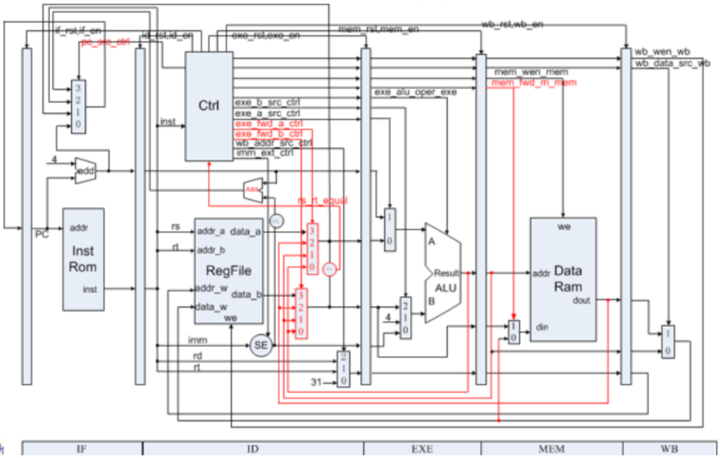
Multicycle MIPS CPU
 Yudai Chen
The CPU supports up to 31 MIPS instructions.
The following is about how did I resolve control hazards & data hazards.
Improve the design of Datapath of 5-stages Pipelined CPU to implement 1-cycle stall when CPU takes Predict-taken policy.
Bring forward calculation of condition & branch address
Bring forward bypass unit.
Basic Principles
Pipelined CPU
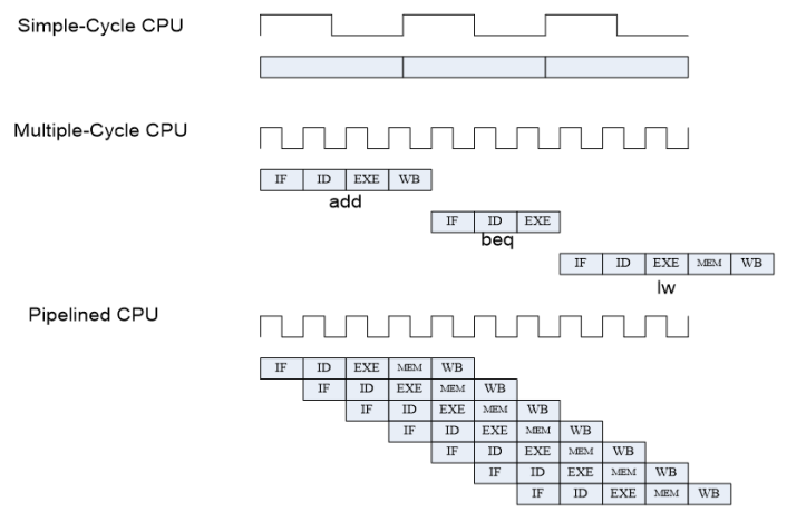
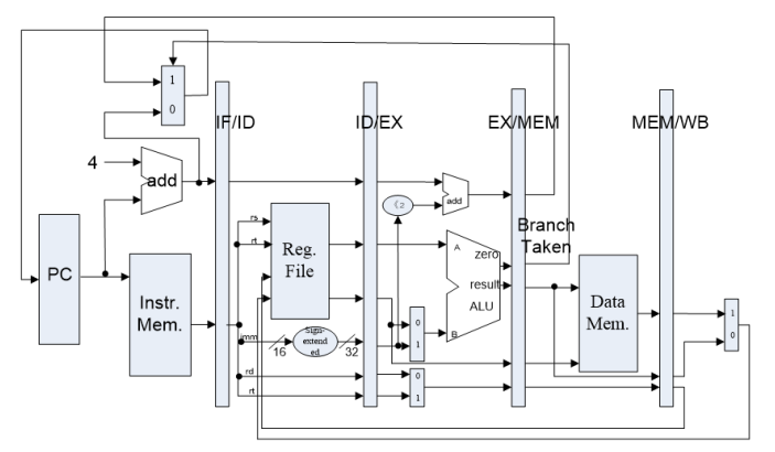
Datapath of 5-stages Pipelined CPU
Data Hazard
Data hazards occur when the pipeline changes the order of read/write accesses to operands comparing with that in sequential executing .
Example:
- DADD R1, R1, R3
- DSUB R4, R1, R5
- AND R6, R1, R7
- OR R8, R1, R9
- XOR R10, R1, R11
Forwarding——Coping with data hazard
The bypass method can reduce data hazard stalls.
Instead of waiting to store the result, we forward it immediately (more or less) to the instruction that wants it.
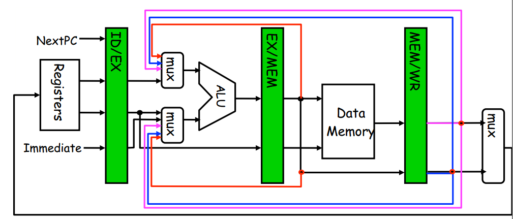
Mechanically, we add buses to the datapath to move these values around, and these buses always “point backwards” in the datapath, from later stages to earlier stages.
There are four cases of forwarding:
Exe/Mem.ALUoutput->ALU input
Mem/WB.ALUoutput->ALU input
Mem/WB.LMD->ALU input
Mem/WB.LMD->DM input
![]()
Forwarding Case
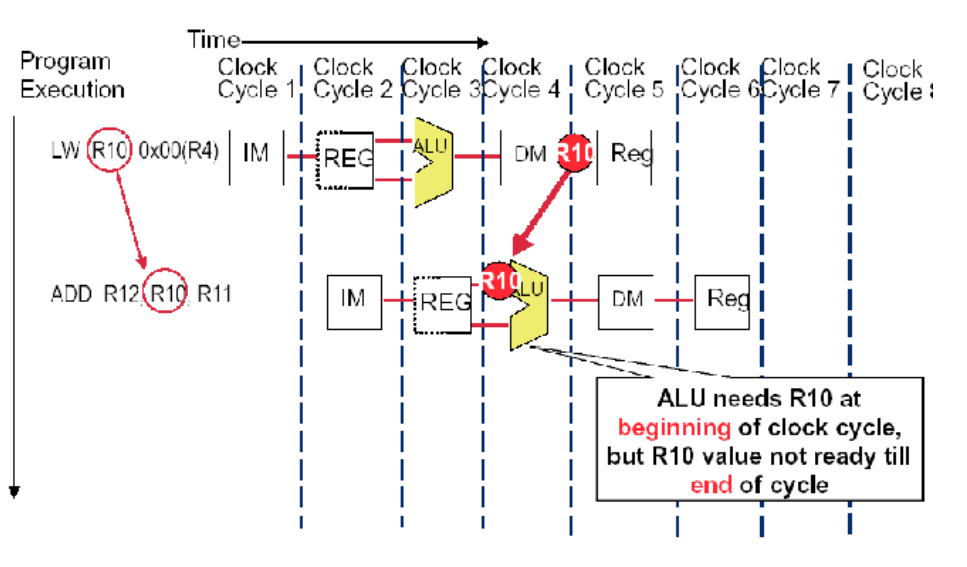
But forwarding does not always work, so we still have to insert stall in some cases (after lw instructions).
In theory, it is necessary to insert a stall. But in actual programming, we do not actually need to insert a stall. Instead, we directly add a line from the output of DM to the input of ALU.
This is because DM takes the value out of the negative edge of the clock, but because the speed of ALU is fast enough, it doesn’t need a clock cycle to do this. Therefore, after the value is taken from DM, ALU can complete the computation in the current cycle, so there is no need to stall.
Delay Slot
Obviously, we can deal with the branch hazard by inserting stalls into the pipeline, but when we do this, the efficiency of the CPU will be reduced greatly.
So this time we apply delay slot. A delay slot is an instruction that must be executed. If there is such an instruction, then This instruction can substitute one stall.
The following is the datapath after resolving control hazards.
My CPU Modules
Controller
![]()
Controller 1 ![]()
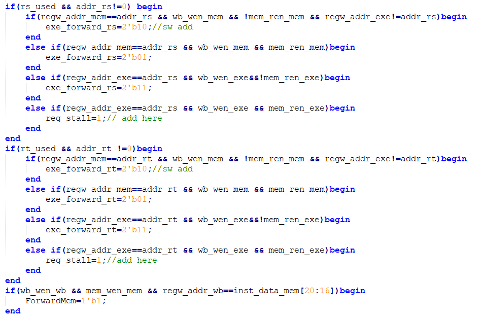
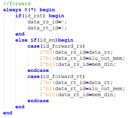
Controller 2 Explanation:
If the instruction at EXE stage is an ALU instruction, stall.
If the write-back address at MEM stage is to be used, forward it.
If the instruction at EXE stage is an lw instruction, stall.
After the just stall, the instruction comes to the MEM stage. If it’s an lw instruction, stall.
If the next instruction is an lw instruction, forward it.
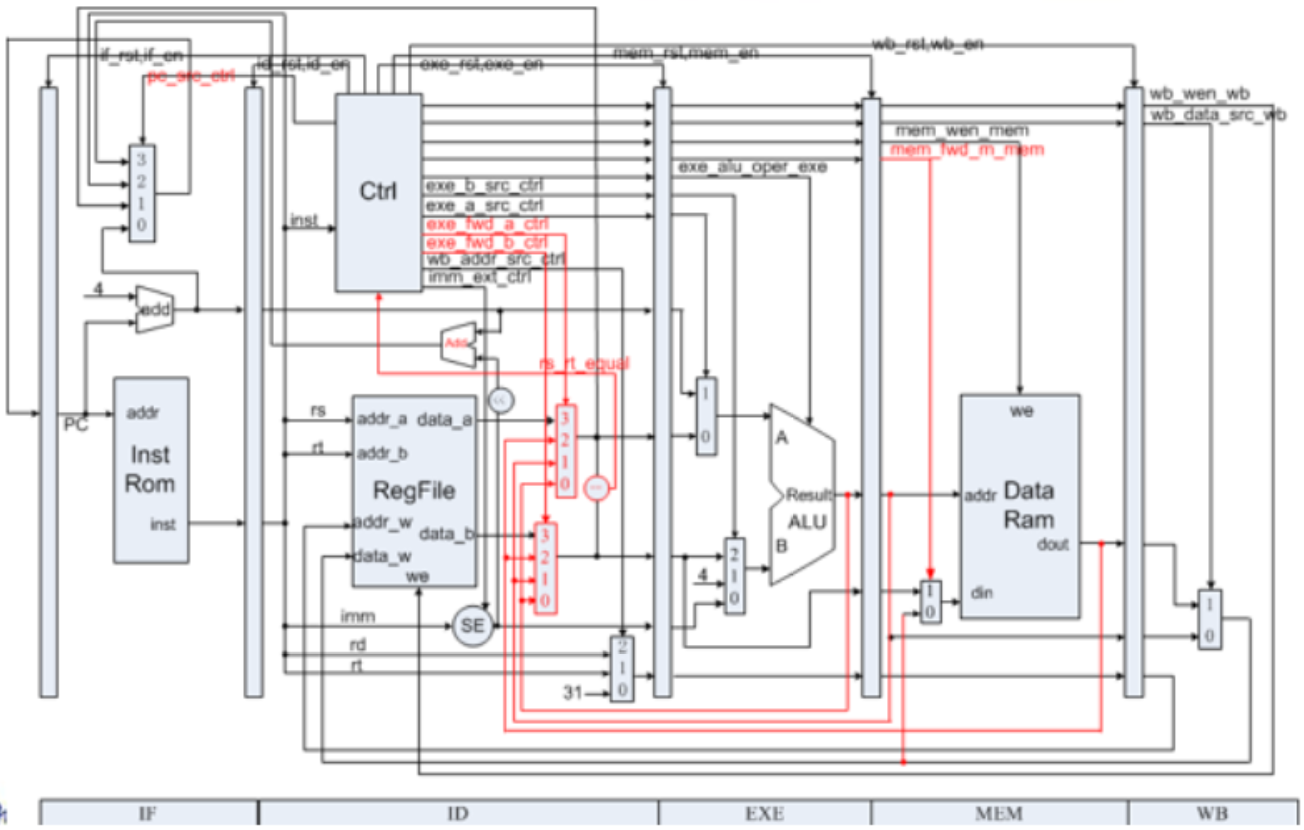
Datapath
![]()
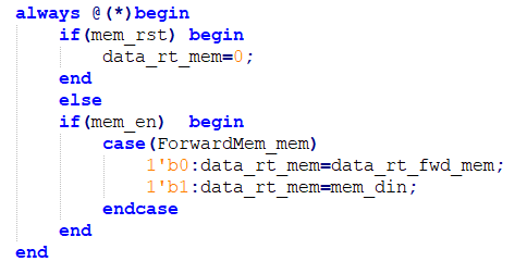
Datapath 1 0 for no need of bypass. 1 for forwarding from alu-out after a stall. 2 for lw instruction, which needs a bypass from mem_din.
Respond for the forward signal at the MEM stage.
![]()
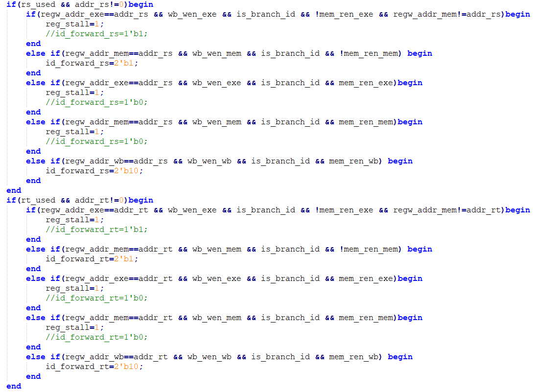
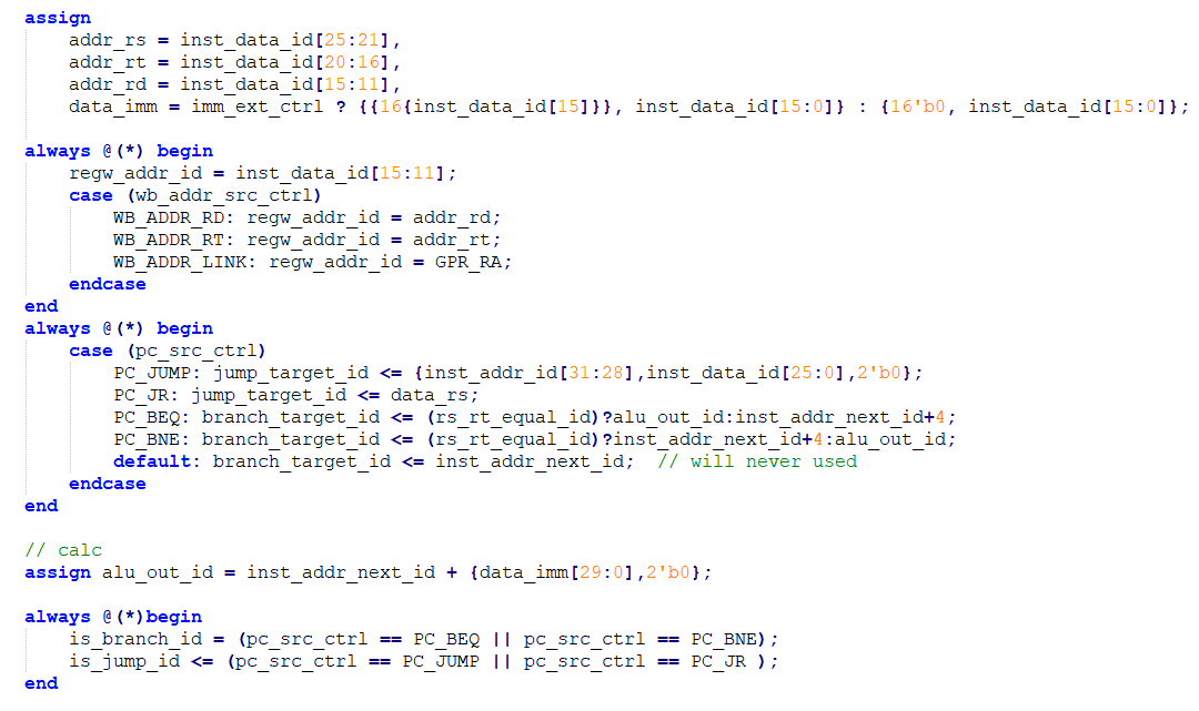
Datapath 2 ID stage:
![]()
Datapath 3 The target address is different between beq and j instruction.
As for jal instruction, the address stored in the $ra register should be changed into PC+8.
![]()
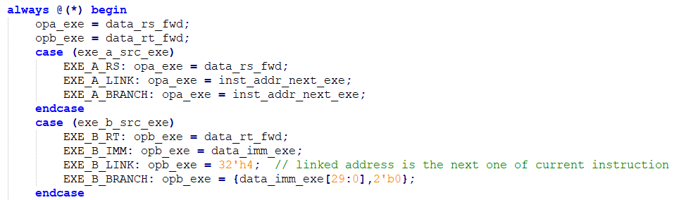
Datapath 4
Experiments
Instruction sequence:
| MIPS Instruction | Explanation |
|---|---|
| and $1, $0, $0 | $1=0 |
| ori $4, $1, 80 | $4=0x50 |
| call: jal sum | jump to sum |
| addi $5, $0, 4 | Delay slot: $5=4 |
| return: sw $2, 0($4) | return label. Save $2 to address stored in $4 |
| lw $9, 0($4) | load 0x258 to $9 |
| sw $9, 4($4) | save $9 (0x258) to the next word from address stored in $4 |
| sub $8, $9, $4 | $8=0x258-0x60=0x1F8 |
| j finish | |
| nop | stall |
| sum: add $8, $0, $0 | $8=0 |
| loop: lw $9, 0($4) | $9=A3 |
| add $8, $8, $9 | $8=A3 |
| addi $5, $5, -1 | $5=3 |
| addi $4, $4, 4 | $4=0x54 |
| slt $3, $0, $5 | $3=1 |
| bne $3, $0, loop | Each loop extract number from RAM and add it to $8. Extract sequence: A3, 27, 79, 15 |
| addi $4, $4, 4 | Delay slot: $4+=4 |
| jr $ra | return |
| or $2, $8, $0 | Delay slot:$2=$8=0x258 |
| nop | stall |
In the simulation, the value of $9 is in sequence of 0xA3, 0x27, 0x79, 0x155, 0x258. Finally the value of $8 in theory should be 0x1F8.
Simulation result:
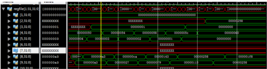
The result of simulation meets the result in the theory. And the execution of the instructions in the delay slot is also correct. When the instruction jal is executed, the value of $ra register is PC+8.
Verification on FPGA board:
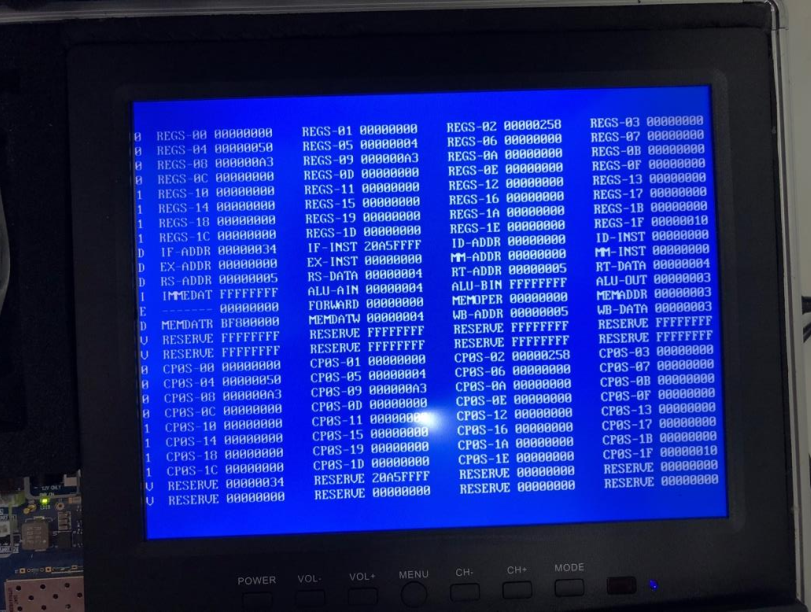
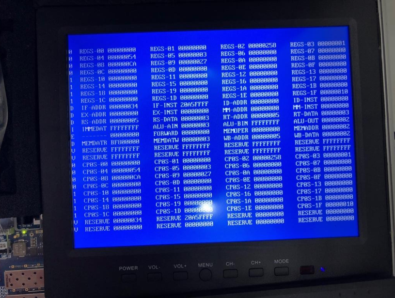

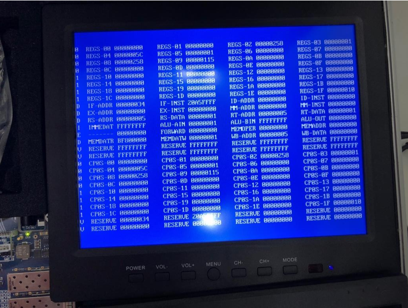
A3、27、79、115 are read from RAM,and added to $8,and the result is correct.
Yudai Chen
Master’s Student at Rice University, former ZJUer
I obtained my Bachelor of Engineering degree in Computer Science from Chu Kochen Honors College of Zhejiang University in July 2019. Currently I’m a master’s student majoring in Computer Science at Rice University. My interests include web development(mainly backend), distributed system, cloud computing, high performance computing, and infrastructure.